Scaling down material synthesis to crystalline structures only a few atoms in size and precisely positioned in device configurations remains highly challenging, but is crucial for new applications, for example, in quantum computing. In a recent study, a NanoLundian research team explores how.
They found that crystal-phase selective Bi incorporation on GaAs nanowires is a result of the interplay between the atomic morphology and the surface energy of the different nanowire facets.
The self-selective formation only on wurzite segments, in combination with the tunability of the structure of the nanowire template, opens the path towards monolayer thin nanostructures with variable width, atomically sharp borders, and promise for exotic electronic phases of matter.
Atomic-scale precision
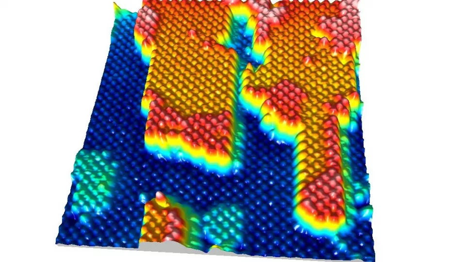
“The study starts with trying to synthesize atomically thin layers of the material gallium bismide (GaBi) on the surfaces of gallium arsenide (GaAs) nanowires. Upon this, we found out that the different exposed crystal planes of nanowire sidewalls can have big impacts on the GaBi growth: Nanowires can crystallize in different crystal shapes, for example, wurtzite and zincblende, due to their small footprint – unlike bulk materials which always have one preferred phase – and in addition, their surface facets look into different geometric directions. Among all types of phases and directions, we found out that wurtzite {11-20} is the most exciting facet because it allows us to grow ordered GaBi nanostructures with atomic-scale precision”, says Yi Liu, Doctoral student at Synchrotron Radiation Research and NanoLund.
Promising for quantum information technology
“So far, GaBi has been considered thermodynamically unstable and bulk GaBi has not been successfully synthesized yet. However, GaBi has been predicted to be a topological insulator and show properties such as band inversion. So, our successfully synthesized GaBi will make it possible to study this material with large potential for new electronic applications: topological insulators are promising for quantum information technology, while GaAs is a classical semiconductor with well-established device platforms. The combination of both opens up for new exciting devices”, Yi Liu continues.
Another very interesting result, from a more fundamental material science perspective, is that the unique wurtzite crystal plane, which only exists on the sidewall of GaAs nanowires, can offer a special growth mechanism when synthesizing 1D and 2D GaBi island which is not available on conventional surfaces.
Unique nanostructures
So, what’s the most important thing with this study?
“We found that crystal-phase selective Bi incorporation on GaAs nanowires is a result of the interplay between the atomic morphology and the surface energy of the different nanowire facets. In our case, by carefully tailoring wurtzite/zincblende heterostructure nanowires, unique 2D and 1D nanostructures of pure GaBi can be achieved, growing self-selectively. A high density of step edges facing [0001]A/B directions is found essential to trigger the controlled Bi incorporation”, says Yi Liu.
Thus, the approach of using tailored nanowire-based templates and radial overgrowth for the realization of well-positioned nanostructures and quantum dots down to atomic scale is valuable and inspiring for other related studies as well.
The results show a new way how to synthesize GaBi, a material that is in the focus of many research groups. Furthermore, the research team shows how nanowires, with atomically precise interfaces, can be used as templates for the synthesis of highly precise devices in the future.
The hunt for smaller and smaller structures
This study may be important to the public because the industry is striving to process smaller and smaller structures in a top-down approach based on complex and very expensive lithography and etching steps.
“This implies that more and more transistors can be built within the same area on a chip. Nowadays the highest precision of commercially available features that chipmakers can offer is 5 nanometers, the so-called “5 nm node”, and it is predicted that the “2 nm node” will come true around 2024. However, while the precision is approaching the size of single atoms (normally in the size of several Å, 1 Å=0.1 nm), the room for improving the precision by complex processing steps is rather limited”, says Rainer Timm, Senior lecturer at Synchrotron Radiation Research and Principal investigator at NanoLund.
“Our approach, however, is a self-organized process based on site-selected formation, utilizing nanowire heterostructures as templates, which can be grown with atomic-scale precision. Combining this unique growth mechanism with the material properties of GaBi, the results of this study lead the way towards nanowire-based devices with atomic-scale precision and novel electronic properties”, says Yi Liu.
The research team was taken by surprise several times during the study:
“We did not expect that Bi growth would be so different on different crystal planes on the sidewall of nanowires. Specially, we did not expect that such nicely ordered GaBi can be generated on Wz {11-20} facet. Later on, after trying to optimize the template, we realized that the density of atomic steps plays an important role here, in addition to the crystal structure itself, which was another surprise”, says Rainer Timm.
The article is written by Yi Liu, Johan V. Knutsson, Nathaniel Wilson, Elliot Young, Sebastian Lehmann, Kimberly A. Dick, Chris J. Palmstrøm, Anders Mikkelsen and Rainer Timm.
Nature Communications volume 12, Article number: 5990 (2021)